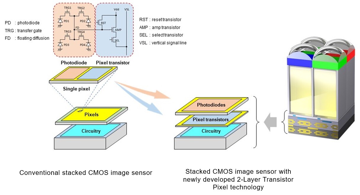
Sony Semiconductor Solutions Corporation has succeeded in developing the world’s first stacked CMOS image sensor technology with 2-Layer Transistor Pixel. Whereas conventional CMOS image sensors’ photodiodes and pixel transistors occupy the same substrate, Sony’s new technology separates photodiodes and pixel transistors on different substrate layers. This new architecture approximately doubles saturation signal level relative to conventional image sensors, widens dynamic range and reduces noise, thereby substantially improving imaging properties. The new technology’s pixel structure will enable pixels to maintain or improve their existing properties at not only current but also smaller pixel sizes.
A stacked CMOS image sensor adopts a stacked structure consisting of a pixel chip made up of back-illuminated pixels stacked atop a logic chip where signal processing circuits are formed. Within the pixel chip, photodiodes for converting light to electrical signals, and pixel transistors for controlling the signals are situated alongside each other on the same layer. Increasing saturation signal level within form-factor constraints plays an important role in realizing high image quality with wide dynamic range.